- 您现在的位置:买卖IC网 > Sheet目录342 > MCP14E9T-E/MF (Microchip Technology)IC MOSFET DRIVER 3A 8DFN-S
�� �
�
�MCP14E9/10/11�
�TABLE� 4-1:�
�ENABLE� PIN� LOGIC�
�MCP14E9�
�MCP14E10�
�MCP14E11�
�ENB_A�
�H�
�H�
�H�
�H�
�L�
�ENB_B�
�H�
�H�
�H�
�H�
�L�
�IN� A�
�H�
�H�
�L�
�L�
�X�
�IN� B�
�H�
�L�
�H�
�L�
�X�
�OUT� A�
�L�
�L�
�H�
�H�
�L�
�OUT� B�
�L�
�H�
�L�
�H�
�L�
�OUT� A�
�H�
�H�
�L�
�L�
�L�
�OUT� B�
�H�
�L�
�H�
�L�
�L�
�OUT� A�
�L�
�L�
�H�
�H�
�L�
�OUT� B�
�H�
�L�
�H�
�L�
�L�
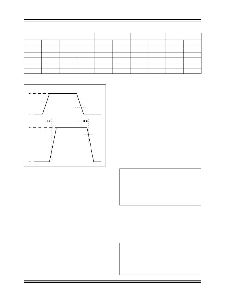
�4.5�
�PCB� Layout� Considerations�
�5V�
�A� proper� PCB� layout� is� important� in� a� high-current,� fast�
�switching� circuit,� to� provide� proper� device� operation�
�ENB_x�
�0V�
�V� EN_H�
�V� EN_L�
�and� robustness� to� the� design.� The� PCB� trace� loop� area�
�and� inductance� should� be� minimized� by� the� use� of�
�ground� planes� or� trace� under� MOSFET� gate� drive� sig-�
�nals,� separate� analog� and� power� grounds,� and� local�
�driver� decoupling.�
�V� DD�
�t� D3�
�t� D4�
�Placing� a� ground� plane� beneath� the� MCP14E9/10/11�
�will� help� as� a� radiated� noise� shield,� as� well� as� providing�
�some� heat� sinking� for� power� dissipated� within� the�
�90%�
�device.�
�OUT� x�
�4.6�
�Power� Dissipation�
�0V�
�10%�
�The� total� internal� power� dissipation� in� a� MOSFET� driver�
�is� the� summation� of� three� separate� power� dissipation�
�elements� (� Equation� 4-1� ).�
�FIGURE� 4-3:�
�Enable� Timing� Waveform.�
�EQUATION� 4-1:�
�P� T� =� P� L� +� P� Q� +� P� CC�
�4.4�
�Decoupling� Capacitors�
�Where:�
�Careful� layout� and� decoupling� capacitors� are� highly�
�recommended� when� using� MOSFET� drivers.� Large�
�currents� are� required� to� charge� and� discharge� capaci-�
�tive� loads� quickly.� For� example,� approximately� 2.0A� are�
�needed� to� charge� an� 1800� pF� load� with� 18V� in� 15� ns.�
�P� T�
�P� L�
�P� Q�
�P� CC�
�=�
�=�
�=�
�=�
�Total� Power� Dissipation�
�Load� Power� Dissipation�
�Quiescent� Power� Dissipation�
�Operating� Power� Dissipation�
�To� operate� the� MOSFET� driver� over� a� wide� frequency�
�range,� with� low� supply� impedance,� a� ceramic� and� low-�
�4.6.1�
�CAPACITIVE� LOAD� DISSIPATION�
�ESR� film� capacitors� are� recommended� to� be� placed� in�
�parallel,� between� the� driver,� V� DD� and� GND.� A� 1.0� μF,�
�low-ESR� film� capacitor� and� a� 0.1� μF� ceramic� capacitor�
�placed� between� pins,� 6� and� 3,� should� be� used.� These�
�capacitors� should� be� placed� close� to� the� driver� to� mini-�
�mize� circuit� board� parasitics� and� provide� a� local� source�
�for� the� required� current.�
�The� power� dissipation� caused� by� a� capacitive� load� is� a�
�direct� function� of� frequency,� total� capacitive� load� and�
�supply� voltage.� The� power� lost� in� the� MOSFET� driver�
�for� a� complete� charging� and� discharging� cycle� of� a�
�MOSFET� is:�
�EQUATION� 4-2:�
�Where:�
�P� L� =� f� � C� T� � V� DD�
�2�
�f� =� Switching� Frequency�
�C� T� =� Total� Load� Capacitance�
�V� DD� =� MOSFET� Driver� Supply� Voltage�
�DS25005A-page� 14�
�?� 2011� Microchip� Technology� Inc.�
�发布紧急采购,3分钟左右您将得到回复。
相关PDF资料
MCP1640RD-4ABC
BOARD REF DES AAAA BAT BOOST
MCP3906AT-E/SS
IC ENERGY METERING 24SSOP
MCP3907T-I/SS
IC ENERGY METER W/OSC 24SSOP
MCZ33198EF
IC TMOS DRIVER AUTO HISIDE 8SOIC
MCZ33285EFR2
IC TMOS DRIVER DUAL HISIDE 8SOIC
MCZ33927EK
IC FET PRE-DRIVER 3PH 54-SOIC
MCZ33937EKR2
IC PRE-DRIVER 3PHASE 54-SOIC
MDN2BL3GRAS
MOTOR BRUSHED DC 2V 2753RPM
相关代理商/技术参数
MCP14E9T-E/SN
功能描述:功率驱动器IC 2A MOSFET Driver RoHS:否 制造商:Micrel 产品:MOSFET Gate Drivers 类型:Low Cost High or Low Side MOSFET Driver 上升时间: 下降时间: 电源电压-最大:30 V 电源电压-最小:2.75 V 电源电流: 最大功率耗散: 最大工作温度:+ 85 C 安装风格:SMD/SMT 封装 / 箱体:SOIC-8 封装:Tube
MCP-14-I9-LL
制造商:YAMAICHI 制造商全称:Yamaichi Electronics Co., Ltd. 功能描述:MatchCon
MCP-14-TI9-LL
制造商:YAMAICHI 制造商全称:Yamaichi Electronics Co., Ltd. 功能描述:MatchCon
MCP1525
制造商:MICROCHIP 制造商全称:Microchip Technology 功能描述:2.5V and 4.096V Voltage References
MCP1525_05
制造商:MICROCHIP 制造商全称:Microchip Technology 功能描述:2.5V and 4.096V Voltage References
MCP1525_13
制造商:MICROCHIP 制造商全称:Microchip Technology 功能描述:2.5V and 4.096V Voltage References
MCP1525I/TO
制造商:MICROCHIP 制造商全称:Microchip Technology 功能描述:2.5V and 4.096V Voltage References
MCP1525-I/TO
功能描述:基准电压& 基准电流 2.5V RoHS:否 制造商:STMicroelectronics 产品:Voltage References 拓扑结构:Shunt References 参考类型:Programmable 输出电压:1.24 V to 18 V 初始准确度:0.25 % 平均温度系数(典型值):100 PPM / C 串联 VREF - 输入电压(最大值): 串联 VREF - 输入电压(最小值): 分流电流(最大值):60 mA 最大工作温度:+ 125 C 封装 / 箱体:SOT-23-3L 封装:Reel